School of Physics research team makes progress in full-scale grain-boundary strengthening of perovskite solar cells
Sep 27, 2022
Peking University, September 27, 2022: Polycrystalline halide perovskite solids have emerged as excellent semiconductor materials for photovoltaics, light-emitting diodes, lasers, and photodetectors because of their ease of production and outstanding optoelectronic properties. The polycrystalline nature of the perovskites usually causes a considerable density of grain boundaries (GBs), which is the interface between two individual homophase crystal grains of the same material that are generally oriented in different crystallographic directions.
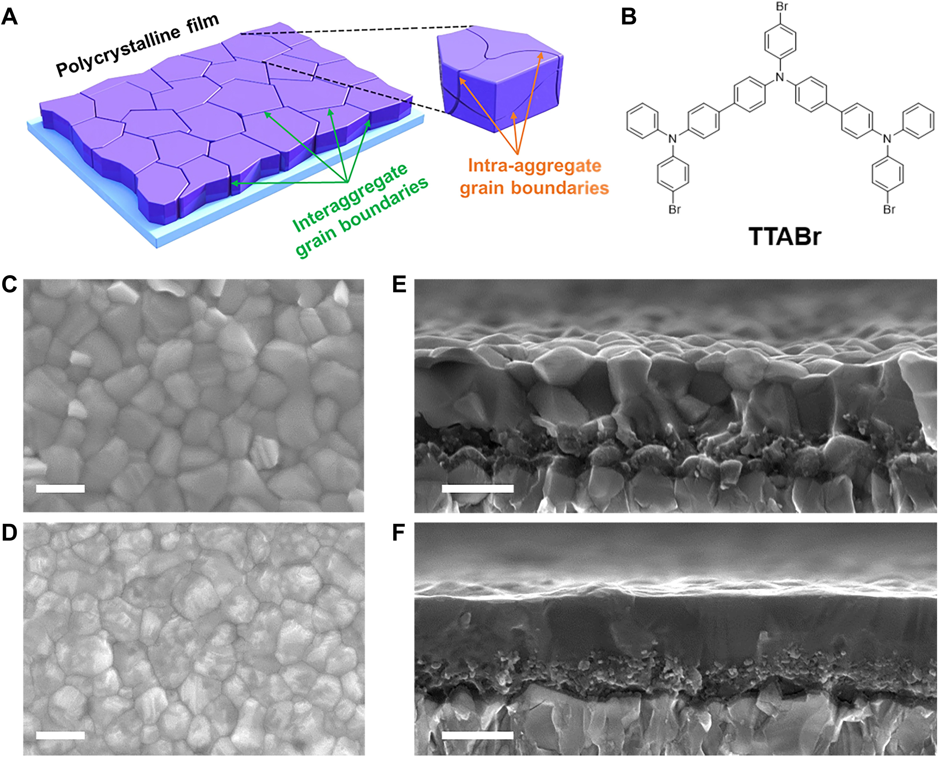
The interaggregate GBs have been frequently and extensively examined in metal halide perovskite research as they can be readily observed by optical microscopy, scanning electron microscopy (SEM), or scanning probe microscopy. By contrast, the number of crystallographic studies on the genuine GBs at the nanoscale and the structural heterogeneity inside grain aggregates by transmission electron microscopy (TEM) is limited to date. Previous studies mainly concerned the interaggregate GBs as they may adversely affect the charge carrier transport, facilitate ion migration, and even produce some deep sub-band energy levels within the bandgap, leading to major nonradiative losses that limit the photovoltaic performance. In addition, some imperfect structures occurring at interaggregate GBs may influence the device stability associated with the presence of mobile charges or ions, oxygen, moisture, heat, and light. In this regard, many approaches, such as surface passivation and functionalization, have been widely studied to suppress these undesirable defects at interaggregate GBs. As such, interaggregate and intra-aggregate GB strengthening is pertinent to enhance the performance of perovskite optoelectronic devices.

Fig. Illustration of solid polycrystalline films and perovskite film morphologies.
(A) Schematic diagram of a solid polycrystalline film with GBs, illustrating interaggregate GBs and intra-aggregate GBs. (B) Chemical structure of TTABr. (C and D) Top-view SEM images of the control (C) and GBMP (D) films. (E and F) Cross-sectional SEM images of the control (E) and GBMP (F) films. Scale bars, 400 nm (C to F).
On September 2, a PKU research team, whose members include Peking University School of Physics researcher Zhu Rui and Dr. Gong Qihuang, published a research paper entitled “Enabling full-scale grain boundary mitigation in polycrystalline perovskite solids” in Science Advances. Their study demonstrated increased regular mesostructured perovskite photovoltaics based on GB-mitigated films with large enhancements in the device efficiency and long-term operational stability under illumination, humidity, or heat stress. The versatility of their strategy is also verified by applying it to different categories of PSCs.
This in-depth structural characterization has not only clarified the existing terminology in the perovskite field but also put forth a new perspective to modulate GBs. This discovery specified a previously unaddressed perspective concerning the full-scale mitigation of GBs in perovskites from the nanoscale to submicroscale, opening a route to obtain high-quality solution-processed polycrystalline perovskite films for high-performance optoelectronic devices.
This research was financially supported by the Beijing Natural Science Foundation, the National Key R&D Program of China, the National Natural Science Foundation of China, the China Postdoctoral Science Foundation, and the R&D Fruit Fund.
Written by: Brenda Cheong
Edited by: Shi Xinyao
Source: PKU News (Chinese)

