Peking University, July 30, 2025: In a landmark advancement for next-generation electronics, researchers from the International Center for Quantum Materials at Peking University in collaboration with Renmin University of China have successfully fabricated wafer-scale two-dimensional indium selenide (InSe) semiconductors. Led by Professor Liu Kaihui, the team developed a novel “solid–liquid–solid” growth strategy that overcomes long-standing barriers in 2D semiconductor manufacturing.
Published in Science under the title “Two-dimensional indium selenide wafers for integrated electronics,” the study demonstrates exceptional electronic performance, surpassing all previously reported 2D film-based devices. The fabricated InSe transistors exhibit ultra-high electron mobility and a near-Boltzmann-limit subthreshold swing at room temperature, establishing a new benchmark for 2D semiconductors.
Background: Why InSe?
Indium selenide, often referred to as a “golden semiconductor,” offers an ideal combination of properties—low effective mass, high thermal velocity, and a suitable bandgap. Despite these advantages, its wafer-scale integration has remained elusive due to the difficulty of precisely maintaining a 1:1 atomic ratio between indium and selenium during synthesis. Traditional methods have only yielded microscopic flakes, insufficient for practical electronic applications.
Why it matters
As Moore’s Law slows and silicon nears its physical limits, the semiconductor industry faces growing pressure to identify alternative channel materials. In this context, the successful fabrication of large-area crystalline InSe wafers represents a pivotal step toward faster, more energy-efficient, and smaller chips for next-generation electronics.
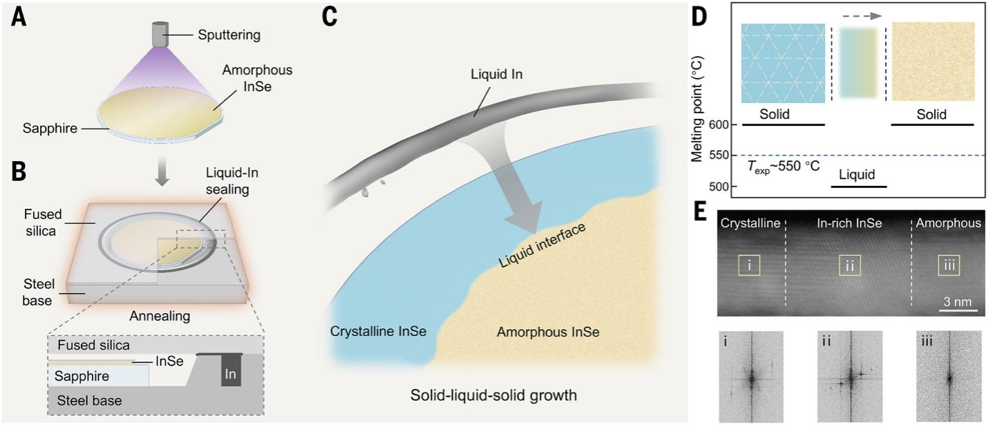
Figure 1. Developing a new “solid-liquid-solid” growth strategy to prepare wafer-level high-quality InSe films.
Key Innovation: Solid–Liquid–Solid Strategy
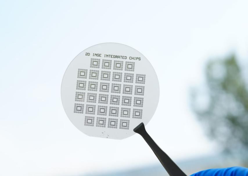
The In–Se system faces challenges due to multiple stable phases and extreme vapor pressure differences between indium and selenium, making it difficult to maintain stoichiometry during growth. These issues hinder phase purity, crystal quality, and overall device stability. Professor Liu Kaihui’s team developed a novel solid–liquid–solid conversion strategy. This process begins with the deposition of an amorphous InSe thin film onto sapphire substrates using magnetron sputtering. The wafer is then encapsulated with low-melting-point indium and sealed inside a quartz cavity. When heated to approximately 550 °C, the indium creates a localized, indium-rich environment that promotes controlled dissolution and recrystallization at the interface. This carefully orchestrated reaction results in the formation of uniform, single-phase crystalline InSe films. This method produced 2-inch wafers with world-first crystallinity, phase purity, and thickness uniformity for 2D InSe.
Device Performance
Using these wafers, the team fabricated large-scale transistor arrays that demonstrated outstanding performance, including an electron mobility of up to 287 cm²/V·s and an average subthreshold swing of 67 mV/dec. The devices exhibited excellent behavior at sub-10 nm gate lengths, characterised by reduced drain-induced barrier lowering (DIBL), lower operating voltages, enhanced on/off current ratios, and efficient ballistic transport at room temperature.
Significantly, the devices surpassed 2037 IRDS projections for delay and energy-delay product (EDP), positioning InSe ahead of silicon in key future benchmarks.
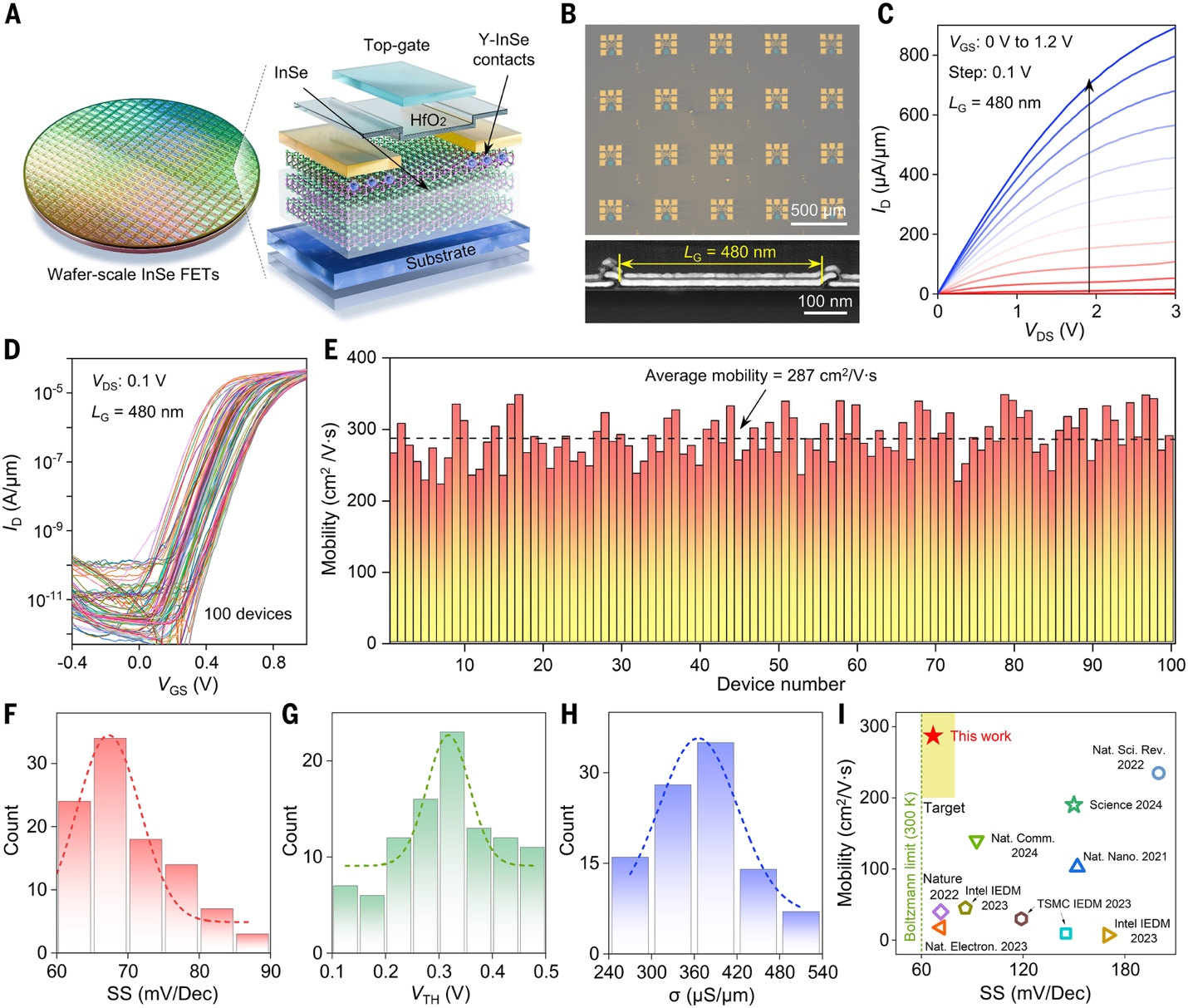
Figure 2. Excellent electrical performance of long channel (AC) and short channel (DF) InSe transistor devices.
Future Implications
This breakthrough opens a new pathway for the development of next-generation, high-performance, low-power chips, which are expected to be applied widely in cutting-edge fields such as artificial intelligence, autonomous driving, and smart terminals in the future. Reviewers of Science have hailed this work as "an advancement in crystal growth."
*This article is featured in PKU News "Why It Matters" series. More from this series.
Read more: https://www.science.org/doi/10.1126/science.adu3803
Written by: Akaash Babar
Edited by: Zhang Jiang
Source:
Xinhua News