Peking University, February 1, 2026: In the era of artificial intelligence (AI), the demand for high-performance, low-power chips is growing rapidly. The conventional von Neumann architecture—marked by the physical separation of memory and computing units—incurs substantial data transfer delays and high energy costs, long confining chip advancement within the so-called "Power wall" and "Memory wall." In this context, nonvolatile ferroelectric materials, capable of fast polarization switching, present a promising pathway toward computing-in-memory architectures. Among them, the ferroelectric field-effect transistor (FeFET), which integrates both logic and memory functions, is considered a key device for building next-generation high-efficiency embedded memory and computing-in-memory chips.
However, its practical application faces a critical challenge: the wafer-scale fabrication of uniform and ultra-thin ferroelectric films. When film thickness is scaled down to 5 nanometers or even the atomic level, the spontaneous polarization of conventional ferroelectric materials degrades significantly, and interface depolarization effects intensify, leading to severe performance deterioration in devices. Therefore, maintaining ferroelectricity at atomic-scale thickness and achieving reliable, consistent wafer-scale integration has become a core problem that must be solved to develop high-efficiency ferroelectric computing-in-memory chips.
On January 29, 2026, a research team led by Professor Peng Hailin from the College of Chemistry and Molecular Engineering at Peking University published a research article online in Science titled "Wafer-scale ultrathin and uniform van der Waals ferroelectric oxide" (
Science 2026, 391, eadz1655). This study reports a novel high-dielectric-constant (κ) van der Waals ferroelectric material, α-phase bismuth selenite (Bi2SeO5). For the first time, the research team realized controlled wafer-scale fabrication of ultra-thin, uniform ferroelectric films and corresponding ferroelectric/semiconductor heterostructures.
Based on this material, they constructed high-speed ferroelectric transistors featuring an ultra-low operating voltage (0.8 V) and exceptionally high endurance (>1.5 × 10¹² cycles). The overall device performance markedly exceeds that of current industrial hafnia-based ferroelectric systems, establishing a new benchmark for ferroelectric transistors in terms of operating voltage, energy consumption, and endurance reported to date. Moreover, the team successfully demonstrated dynamically reconfigurable in-memory logic computing circuits that operate at CMOS-compatible low voltages (<1 V).
This work demonstrates the world's first high-performance wafer-scale two-dimensional ferroelectric material system, offering both a groundbreaking material platform and a viable technological route toward high-efficiency advanced chips. With its strong potential to drive the sustained advancement of AI hardware, this development paves the way for continued progress in achieving higher computational performance coupled with lower power consumption.
 Figure 1. Schematic diagram of wafer-scale van der Waals highκ ferroelectric oxide/high-mobility 2D semiconductor heterostructure and its high-performance ferroelectric transistor device.
Addressing a Critical Industry Bottleneck: The Challenge of Fabricating High-Quality Ferroelectric Materials
Figure 1. Schematic diagram of wafer-scale van der Waals highκ ferroelectric oxide/high-mobility 2D semiconductor heterostructure and its high-performance ferroelectric transistor device.
Addressing a Critical Industry Bottleneck: The Challenge of Fabricating High-Quality Ferroelectric Materials
With the rapid advancement of technologies such as AI, cloud computing, big data, and 5G, the demand for higher chip performance continues to grow. The decades-old von Neumann architecture, which separates computing from memory, severely limits improvements in system energy efficiency. Ferroelectric materials, owing to their "spontaneous polarization" property, are regarded as key to breaking through the conventional architecture and building next-generation computing-in-memory chips. FeFET ingeniously integrates memory and computing functions within a single device, endowing the transistor with "memory" capability. This fundamentally eliminates the energy consumption and latency caused by frequent data movement, making FeFETs particularly suitable for advanced architectures such as computing-in-memory and neuromorphic computing.
However, to achieve practical applications compatible with advanced process nodes, a key bottleneck must be overcome: the uniform fabrication of high-quality ultra-thin ferroelectric films. Although mainstream hafnia-based ferroelectrics are compatible with silicon processes, they still face issues of insufficient uniformity and degraded ferroelectricity when scaled to wafer-level, ultra-thin dimensions. Therefore, there is an urgent need to develop new ferroelectric materials that combine wafer-scale uniformity, stable ferroelectricity at ultra-thin thicknesses, and high compatibility with semiconductor manufacturing lines. This will truly unlock the potential of computing-in-memory chips and accelerate their transition from the laboratory to large-scale industrial application.
Video: Wafer-scale ultra-thin uniform ferroelectric αBi₂SeO₅ film and ferroelectric transistor.
Developing Core Material Innovations: A Novel Bismuth-Based 2D High κ Ferroelectric Oxide
To break through the constraints of the “Power wall” and “Memory wall” imposed by conventional chip architectures, the research group led by Peng Hailin at Peking University has long been committed to exploring new material systems suitable for post-Moore nonvon Neumann advanced chips. As early as 2018, the group first identified the native oxide of bismuth-based 2D semiconductor Bi2O2Se—αBi2SeO5—and theoretically predicted its ferroelectricity. However, the path from theory to experimental confirmation is long and challenging. Due to multiple bottlenecks in materials, devices, and characterization, this prediction remained experimentally unverified for years.
After nearly eight years of persistent effort, the group has now experimentally confirmed the ferroelectricity of αBi₂SeO₅ for the first time. Moreover, they have developed a back-end-of-line-compatible (≤400 °C) in-situ oxidation fabrication method that enables wafer-scale, uniform synthesis of ultra-thin ferroelectric films (Fig. 1). Owing to its unique van der Waals layered structure, αBi₂SeO₅ retains stable ferroelectricity even down to a mono-layer thickness, making it an ideal material for atomic-scale nonvolatile memories and sub5nm three-dimensional computing-in-memory architectures. This breakthrough opens new possibilities for pushing beyond the current performance limits of integrated chips.
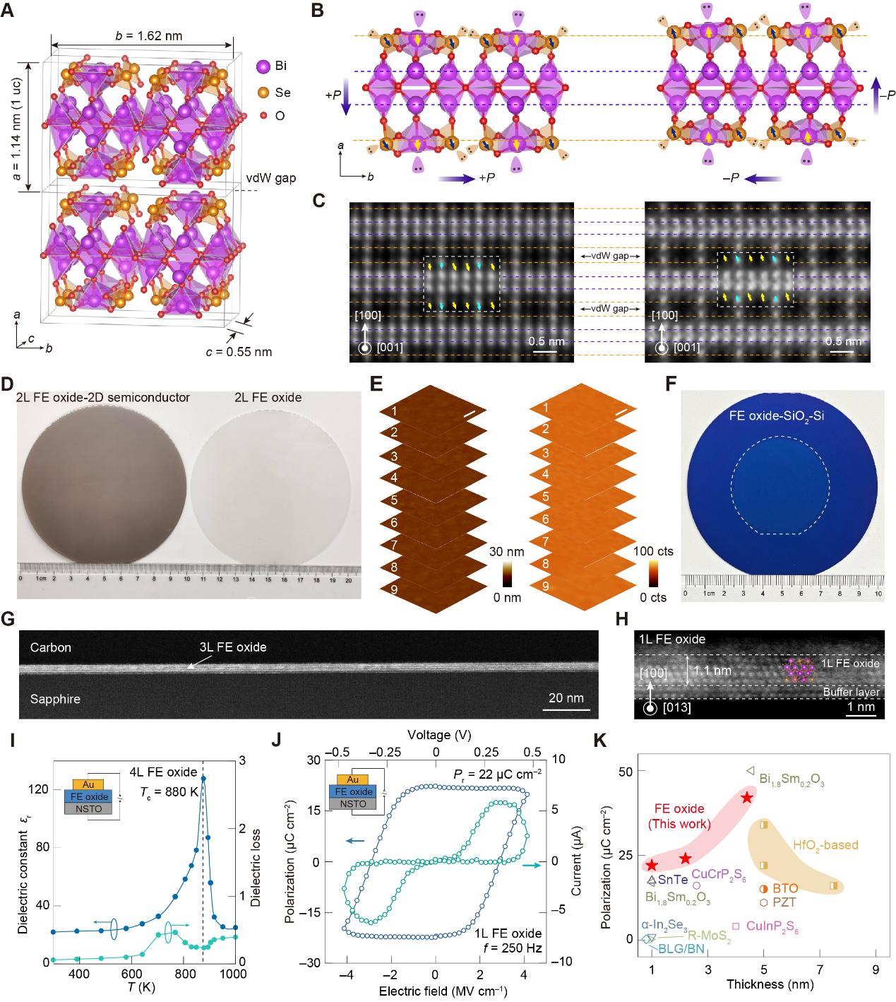
Figure 2. Waferscale uniform fabrication and ferroelectricity of the two-dimensional high κ ferroelectric oxide αBi₂SeO₅.
Pushing Device Performance Limits: A 2D Ferroelectric Transistor and Circuit with Ultra-low Operating Voltage and High Endurance
This work has further fabricated high-performance ferroelectric transistor arrays (Fig. 3). Operating at an ultra-low voltage of 0.8 V with a fast 20 ns write speed, the device demonstrates exceptional endurance exceeding 1.5 × 10¹² cycles, a retention time of 10 years, 5bit multilevel storage capability, and an ultra-low energy consumption of 2.8 fJ bit−1 μm−2. These metrics surpass the highest industrial standards for memory devices and fully meet the stringent reliability requirements for cloud computing. By overcoming the conventional trade-offs in ferroelectric materials between retention and endurance, as well as between speed and energy consumption, this work provides a highly promising solution for low-power, three-dimensionally integrated computing-in-memory architectures tailored to AI computing demands.
Furthermore, the fabricated dynamically reconfigurable logic-in-memory circuit (Fig. 4) can perform switchable logic operations under CMOS-compatible low operating voltages (<1 V). This clearly demonstrates its significant potential for next-generation computing-in-memory architectures and lays a critical device-level foundation for building adaptive, low-power intelligent computing systems.
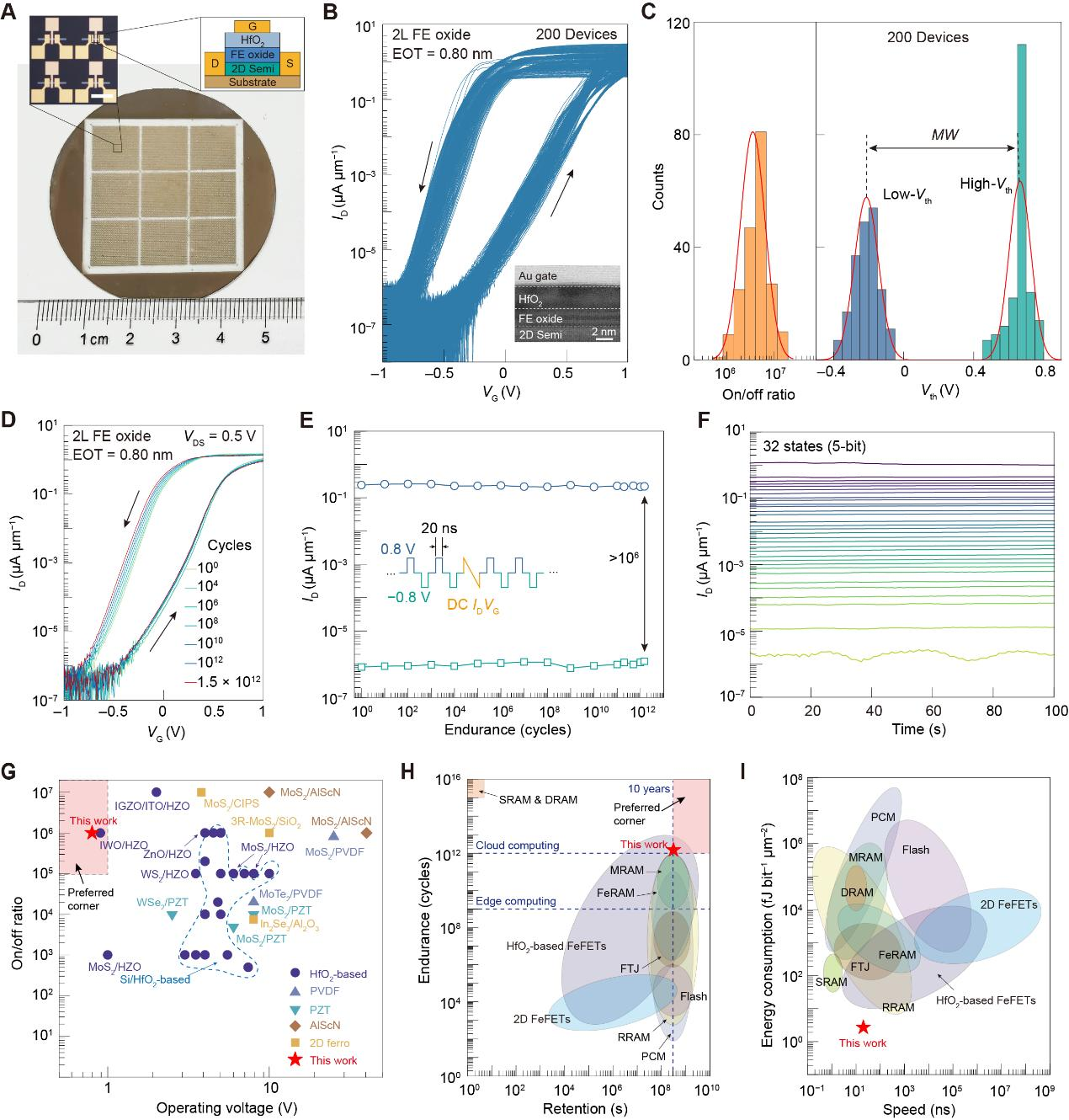
Figure 3. Device structure and performance of the 2D α-Bi2SeO5/Bi2O2Se ferroelectric transistor.
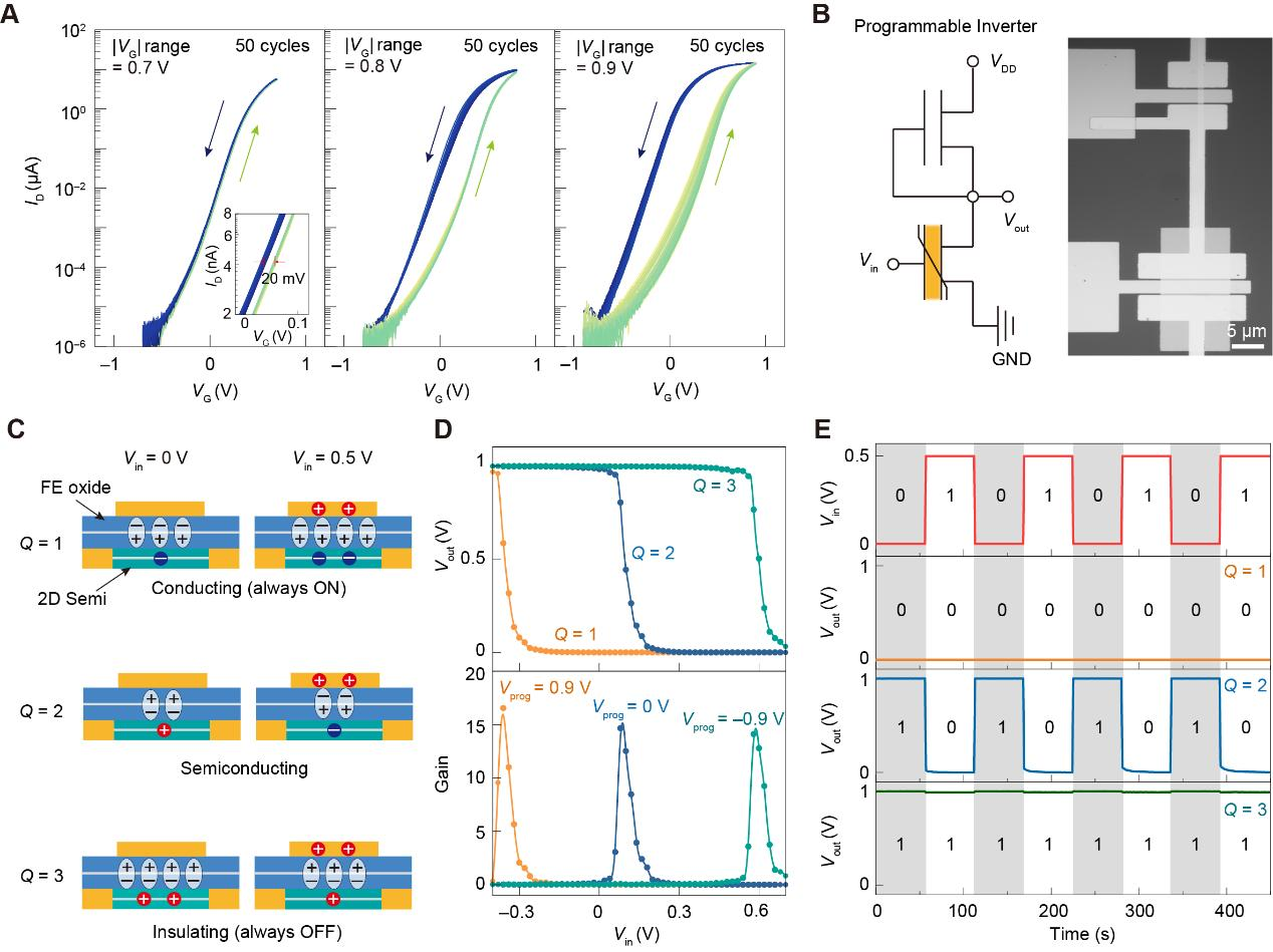
Figure 4. Low-power reconfigurable logic-in-memory circuit based on 2D α-Bi2SeO5/Bi2O2Se ferroelectric transistors.
Reviewers commented: "Not only does this work overcome the thickness-scaling limitations of traditional ferroelectrics and the wafer-scaling limitations of 2D ferroelectrics, but it also opens the door toward realizing ferroelectric-based 2D electronics, considering Bi2SeO5 is a native oxide for its semiconducting sister compound Bi2O2Se. The authors also report outstanding memory performance and low variability in ferroelectric field effect transistors." They further stated, "This work will be extremely impactful to both the ferroelectric materials community as well as the ferroelectric device community."
In summary, this study represents the first worldwide realization of wafer-scale, ultra-thin, uniform 2D ferroelectric oxide films and three-dimensional heterogeneous integration with 2D semiconductors. It has also led to the development of ferroelectric transistors and reconfigurable logic-in-memory circuits that feature ultra-low operating voltage and record-high endurance. By simultaneously advancing the frontiers of ferroelectric material synthesis and device performance, this work provides a new material platform and integration strategy for next-generation high-performance, low-power chip technology. It marks a significant leap along the "More than Moore" road map—from material innovation to full functional demonstration.
Read more: https://www.science.org/doi/10.1126/science.adz1655
Edited by: Chen Shizhuo
Source: College of Chemistry and Molecular Engineering